
Aug 27 2025
Quality and Me (Part I) — Semiconductors
This is the first of several posts about my personal history with manufacturing quality. While I have never had the word “quality” in my job title, and it has never been my exclusive focus, I can’t name a project I have worked on in the past 44 years that didn’t have a quality dimension.
Controversial views about quality have earned me rebukes from quality professionals, who gave me reading lists. To see the error of my ways, all I had to do was study the complete works of Walter Shewhart, W. Edwards Deming, and Donald J. Wheeler. It never occurred to them that I might be familiar with these authors.
There are also other authors on quality that my contradictors ignored or dismissed, like J.M. Juran, Kaoru Ishikawa, or Douglas Montgomery. I didn’t see them as any less worthy of consideration than the ones they were adamant about.

I don’t think any of these authors intended their works to be scripture. Instead, they aimed to assist their contemporaries in addressing their quality issues with the technical and human resources available. We should do the same today. I recently heard from Sam McPherson of a piece of advice haiku author Matsuo Bashō gave to a painter in 1693: “Do not follow the footsteps of the ancients, seek what they sought instead.” This is what I have been doing.
Contents
Japan, 1980
Francis Lecroisey, a scientific attaché I was working for at the French embassy in Tokyo, first drew my attention to Japanese quality achievements in automotive, electronics, or shipbuilding, and to two Americans, Deming and Juran, who, along with Kaoru Ishikawa, had played a key role 30 years before in starting the transformation that had led to this situation.
Deming was already 80 years old but had yet to publish his currently most cited books, Out of the Crisis (1986) and The New Economics (1992). The NBC special “If Japan can, why can’t we?” that lifted Deming out of obscurity in the US had just aired, but I hadn’t seen it. It was the dawn of the VHS era, and videos didn’t circulate as freely as they do now. Juran had a more substantial paper trail: his Quality Control Handbook was already on its 3rd edition (1974).
Kaoru Ishikawa had written several books promoting QC circles (1962), and defining the technical training of QC circle members (1970). His book on the Japanese version of TQC was published in Japanese in 1981. Norman Bodek had started Productivity Press a year before and would make Japanese books about manufacturing available in English through the 1980s.
Lecroisey also introduced me to Prof. Naoto Sasaki, who taught Quality at Sophia University and later played a pivotal role in my becoming a consultant by introducing me to Kei Abe. In our conversations, he warned me not to exaggerate the impact of QC circles. Yes, they contributed, but there was much more that needed to be done. If QC circles were all you did, you couldn’t get far.
His nuanced perspective, however, did not resonate with the American or European public. In today’s terms, QC circles went viral and many companies started using them. Within about two years, they went out of fashion, never to return. Today, the only factories in the US with anything resembling QC circles are Japanese transplants. In the Asia-Pacific region, on the other hand, QC circles have taken root and are part of quality management in many companies.
Silicon Valley, 1980s
In 1981, I stepped into the manufacturing arena. I moved to the US and started as a process engineer at Fairchild Semiconductor. All I knew about making integrated circuits (ICs) was an article I had read in Scientific American. So I crammed and asked questions.
My last project in this industry was 31 years ago, and it has, of course, massively changed since. The industry leader then was Intel, and it made the chips it designed. The leading company in 2025 is NVIDIA, which only designs them. Taiwan’s TSMC then manufactures the chips and has the most advanced process technology.
Per what TSMC advertises on its own methods for yield enhancement, they are based on AI, machine learning, and Advanced Process Control (APC), which is the continuation of industry practices from 30 years ago with more powerful means addressing tougher technical challenges.
But I am not trying to advise anyone on quality issues in the semiconductor industry today. What I am sharing instead is how the reality of this industry challenged my beliefs about quality when I encountered it. Working later in other industries, I found these beliefs challenged again, in different ways. I will cover my experience with aerospace and automotive in the later posts in this series.
Aluminum versus Copper
One question I remember in particular was why the interconnections in Integrated Circuits (ICs) were in aluminum, when copper was a better conductor. The man I asked was Harry Sello, and he had been in the room when IC inventor Bob Noyce had made that choice in 1959.
“Copper,” Sello told me, “doesn’t stick to Silicon. It makes a weak bond and peels off. Aluminum, on the other hand, forms a strong metal bond with silicon.” Noyce’s rival, Jack Kilby at Texas Instruments, had successfully built multiple transistors in on a single germanium crystal, but connected them by soldering on copper wires, which made the result short of a fully integrated circuit. With Aluminum, you could deposit a film on top of a silicon circuit and etch away the unneeded parts to leave the desired network of interconnections. It was a seminal breakthrough for the industry.


49 years later, in 1998, Lisa Su, at IBM, succeeded in making chips with copper interconnections that were 20% faster than with aluminum, but that technology is only used in a few high-end chips.
Wafers
66 years later, integrated circuits are still fabricated on monocrystal silicon wafers, like Noyce’s. His had a diameter of 1 in; today’s wafers, 10 in. Each wafer carries hundreds of circuits, called “die” through fabrication. At the end of the process, you cut the wafers into dies, and package each die into chips.

In 2025, the company with the most advanced technology is Taiwan Semiconductor Manufacturing Company (TSMC), and its logo is revealing. Not only does it show a wafer and dies, but a few of the dies in it are marked in black, suggesting they are defective:

That a less-than-perfect wafer could be used in the logo of an industry leader says much about the quality issues of the semiconductor industry.
Quality Issues in Semiconductors
As I learned the basics of solid-state diffusion, ion implantation, thin-film deposition, photolithography, etching, and many other operations that were strung together in a long sequence to build circuits on silicon wafers. I was also struck by the magnitude of the industry’s quality problems.
Market pressure made chipmakers start high-volume production with a yield of 10%. Per Deming, you should never do that. Later, in Out of the Crisis, he would bemoan “the failure of management to listen to the results of tests, being too eager to put a new product on the market before the competition beats him to it.” (p. 315).
In the semiconductor game, as played by industry leaders, if you waited until you had a capable process, the competition did beat you to the market, and you were at best an also-ran. As management saw it, there was a time window in which to launch a product. If you missed it, it was irrecoverable.
Starting with an output that was 90% defective, manufacturing was in a race to increase the yield. However, when yields reached 60% to 70% three years later, the product was obsolete and you started over with the next generation. At no point in a product’s life was it made with a process that was capable in the statistical quality sense of the word.
Intel co-founder Gordon Moore had predicted in 1975 that the number of transistors on a chip would double every two years. This had become known as Moore’s Law, and the industry made it a prophecy to fulfill. Each company had its own army of yield-enhancement engineers, working to improve quality, but with no connection to the quality department.
Particle Contamination
Some of their methods were surprising. For example, a common cause of defects was particle contamination. Particles floating in the air landed on the wafers, killing the circuits.
Protecting the wafers
The immediate countermeasures were straightforward:
- Produce in clean rooms, with filtered air and elevated pressure, to make the inside air flow out through openings rather than outside air flow in. Since then, cleanliness specs have become ever tighter, and the industry developed SMIF pods to transfer wafer lots between machines without exposing them to ambient air.
- Dress operators in smocks, goggles and gloves to protect the wafers from particles shed by human bodies. These are now full-body suits that take 10 to 15 minutes to put on and take off, and put a damper on shop floor visits by managers.
Shrinking the die
The next step was not so obvious. Wafers were assumed to have a uniform defect density lambda, based on which a die of area A would be particle-free with probability e^{-lambda A}. Therefore, if it was 50% and you shrank the die area by 20%, you would (1) make 16% more dies per wafer and (2) the smaller die would be particle-free with a probability of 87%. The production of defectives due to particles would go down from 50% to 13%, simply because the smaller dies were more likely to dodge the particles.

Shrinking dies, however, was a major engineering effort that you couldn’t do too often, and the smaller dies were also vulnerable to smaller particles And particles were not the only source of defects. You also had misaligned patterns, wrong film thicknesses, skipped steps, and many others.
In 2025, the industry is still dodging point defects that it deems inevitable. Shrinking the die, however, is not the only strategy. It builds the latest chips used for AI with redundant circuitry. For the chip to work, you only need one of these circuits to be defect-free, and, after testing the whole chip, you disable all the other replicas.
Process Controls
The production machines had embedded controllers executing recipes that involved, for example, moving a boatload of wafers into a process chamber, raising the temperature to 1,200ºC, flowing gases into the chamber for 10 hours, cooling down the chamber, and pulling out the boatload of wafers.
The embedded controllers executed recipes but did not hold any information about the effect of these recipes on the wafers. The state of the art in 2025 is to maintain a digital twin of the wafers in process and use it to drive the equipment.
Between operations, you took measurements and visually inspected the wafers. While these steps could detect gross deviations from specs, they were poor predictors of final yields. You could have wafers with the right linewidths, film thicknesses, and sheet resistivities, passing all visual inspections, and still producing dies that failed at Final Test.
Scrubbing Wafers
One method used to salvage wafers contaminated with too many particles was to scrub them mechanically before cleaning them up chemically. This was a rework operation that the engineers would have gladly eliminated, as they didn’t think it was likely to produce high-yielding wafers. A project I undertook was to confirm that the functional test yields of scrubbed wafers were lower than the others.
Manual Data
Operators entered the data manually on paper travelers, which I sifted through to find two groups of wafers, scrubbed and not scrubbed, but having otherwise undergone the same process in the same lots. I was able to retrieve data on tens of wafers for each group and found that the scrubbed wafers had higher yields than the others, suggesting that scrubbing should become part of the standard process!
A Surprising Result
The result was unbelievable, and nobody believed it. It contradicted the expectations of all my colleagues, as well as my own. Yet this was the story that the data staring at me was telling. In retrospect, I suspect sampling bias among the scrubbed wafers. In any case, the evidence was up against our confirmation bias. As the new kid on the block, I lacked credibility.
To test the significance of the difference between the two groups, I had used Binomial Probability Paper, a graphic method invented by Mosteller & Tukey in 1949, which I had learned in a Japanese quality textbook. No one around me knew it, let alone trusted it.
Rejection of the results
Perhaps the data was wrong, but I had no practical way to verify it, so I let it go. What this experience made clear to me was that my colleagues did not analyze data. Their approach to problem solving was what Kaoru Ishikawa summarized as “experience, intuition, and guts”:
- Experience said, “We’ve always done it this way.”
- Intuition said, “I have a feel that this is the solution.”
- Guts said, “I’ll take my chances on this. You bet to win.”
Analyzing data in that context meant turning every page of handwritten records, and this kind of patient work was not valued in that factory.
Test Probes
I had a more successful go at it on a different production line a few months later in a division that made early solid-state cameras from Charge-Coupled Devices (CCDs), sold to the US Air Force as dashcams for jetfighters. One of the final tests was called “V to Light Shield.” After being at 100%, the yield of this test had suddenly dropped to the 40% to 60% range.
From the paper records of the past 6 months, I found that the V to Light Shield test yield had originally been in the same 40% to 60% range as today, had jumped to 100% and stayed there for about 3 months, before dropping back down. This pattern was consistent with the tester having malfunctioned for 3 months, passing every unit because its probes failed to touch it.
In this case, analyzing the data had solved the problem but embarrassed the management team. When the yield had jumped to 100% five months before, no one had realized that it was too good to be true. There were many other tests, and they had taken this jump as good news about one of them.
Three months later, after the tester had been serviced, the probes again made contact with the devices under test, and the yields dropped back down to where they should have been all along, but the bad news caught the attention of the engineers and started a wild goose chase for a root cause in the process. This was not the sort of incident you want to publicize.
Test Data Analysis
At the end of the wafer process, in an operation called Wafer Sort, you test all the chips on each wafer that has made it through the fabrication marathon and decide which ones are worth packaging. You cut up the wafer into individual dies and package the selected ones. Then you put them through Final Test, before shipping them to customers, hoping they don’t return with a Quality Problem Report (QPR).

While measurements and inspections made during wafer fabrication provided a trickle of data with limited predictive power on the function of completed dies, the test operations generated hundreds of variables about each die.
Until the late 1970s, the industry had used testing exclusively for sorting good dies from bad, and had “dumped the data on the floor.” Randall A. Hughes, at Fairchild Test Systems, had the idea of the Integrator, a machine that acquired this data instead, so that it could be used to diagnose the process.
Test Data Analysis in the 1980s
Today, multiple semiconductor equipment makers sell systems to store test data in databases and analyze them for opportunities to tweak the fabrication process and enhance its yield. The engineers then run experiments to validate these opportunities.
The yield enhancement engineers applied the latest multivariate techniques to the test data, none of which were taught as part of Statistical Quality Control. In the early 1980s, they were based on old theories that hadn’t been used at scale when invented for lack of computing power, like Principal Component Analysis (PCA), Factor Analysis (FA), or Linear Discriminant Analysis, which go back to the generations of Karl Pearson, Fisher, or Hotelling.
Today, they include techniques developed in the last 40 years and generally known as Machine Learning. These were created specifically to leverage the rising computing power that is available, thanks to… the semiconductor industry.
Test Data Analysis Today
By the end of the 1980s, semiconductors and pharmaceuticals were the largest industrial markets for the then dominant suppliers of advanced analytical software, RS/1 and SAS. Researchers in pharmaceuticals used these tools to discover new drugs; semiconductor engineers, to enhance yields.
Today, SAS is still a player in data science, but RS/1 has disappeared. The chipmakers developed their own yield enhancement tools on top of these generic software products. In the early 1990s, Motorola Semiconductors let instrument maker KLA Tencor market the yield analytics they had developed with SAS to the industry at large. Their reasoning was that their competitive advantage lay in the skills of their engineers, not in possessing the software. Since then, software tools for data science have proliferated and expanded in scope, but the skills of their users remain key.
Contradiction with the Quality Literature
The literature on statistical quality discourages the use of any technique beyond histograms and control charts. Yet, combined with Ph.D.-level knowledge of process physics and chemistry, the most advanced multivariate analysis tools have been the bread and butter of semiconductor yield enhancement for decades.
At first, I thought the yield enhancement engineers were using overly complex methods that were cures in search of diseases when the simple tools would solve “95% of the problems,” as I had been led to believe. Later in the decade, I had the opportunity to work with HP’s semiconductor division and with Intel, and their continued success at making Moore’s Law happen opened my eyes to the fact that the most advanced tools were actually needed.
Failure Analysis
The parts returned from customers with QPRs were sent for failure analysis to a separate department, where engineers stripped the chips layer by layer all the way back to raw silicon. The chipmakers did this to comply with customer requirements.
By the time defective chips arrived back at the supplier, 4 months had passed since the chips had undergone the operations that had introduced the defects. Since then, these operations usually had been through more than one engineering change, and any recommendation based on failure analysis came too late to be useful.
In terms of quality improvement, the failure analysis department was ineffective. It existed only to humor customers. This was the first example I encountered of activities by a quality department that had no bearing on product quality but were conducted to comply with external mandates.
Pushing SPC in Wafer Fabrication
By 1981, Randy Hughes was building a Manufacturing Execution System (MES) with the ambition of supporting yield enhancement based on the analysis of test data. I joined his group and, among other projects, worked with Zahra Ardehali on an SPC module for wafer fabrication.
From the structure of the process, there were clearly several layers of variability in the measured characteristics:
- Within wafers
- Between wafers within a lot
- Between lots
- Between machine loads that included multiple lots.
We were trying to provide charting tools that would reflect groupings of values based on this structure. While process engineers were interested, the quality department pushed back because our approach violated the SPC standards set in the Western Electric Statistical Quality Control Handbook in 1956, before wafer fabs existed.
We then understood that their primary concern was that outsiders should see charts they recognized. Unlike process engineers, solving problems and enhancing yields was not their primary goal. Here is an example of the charts we produced in 1984:

The standards enforcers couldn’t object to these charts. It even included the meaningless interpolation between consecutive points that Shewhart had omitted from his charts. The problem was that we could not get the engineers to use these charts to troubleshoot their processes.
Current Approach to Supervisory Control
The embedded control system of each machine is supposed to keep the process on target, not compensate for a high or low value of any characteristic by tweaking a later operation. Yet this is exactly what Run2Run controls do. Supervisory Control And Data Acquisition (SCADA) systems exchange data with multiple machines. If the thickness of a film is on the high side on one wafer, it can tell the etcher to work just a bit harder to remove it where needed.
Run2Run controls date back to the early 2000s and is now common in the industry. The infrastructure for it emerged in the latter part of my involvement with the industry. HP had shared with the industry a Semiconductor Equipment Communication Standards (SECS) it had developed internally in the 1970s. Equipment manufacturers gradually adopted it in the 1980s. Based on SECS, the semiconductor industry and its equipment suppliers then agreed on a Generic Equipment Model (GEM), published in the 1990s, which enabled features such as Run2Run.
The key point is that Run2Run is a widely applied approach to supervisory control that is neither technically nor philosophically aligned with SPC.
Engineering changes
When successful, data analysis leads to engineering changes in the fabrication process, which present many challenges:
- The managers in charge are justifiably wary of unintended consequences.
- The changes need to be implemented promptly to increase yields as soon as possible.
- The system needs to maintain traceability.
On paper, an engineer submitted an Engineering Change Request with supporting documentation and routed it through a list of approvers. If approved by all, the team in charge of the master data incorporated the change into the process and archived the previous one. With paper travelers, it was impractical to change an operation for wafers already in process, and therefore, the new process only applied to new starts.
Relying on the company’s internal paper mail would take weeks. Engineers could cut the approval cycle to days by hand-carrying a change request to all stakeholders and making a personal pitch to each. In an emergency, they could call them into a meeting to review and approve the change. And, sometimes, they would ignore the bureaucracy, break the rules, and implement a change without authorization.
Aperture in Photolithography
One engineer, for example, took it upon himself to increase the aperture setting on photolithography equipment to reduce the exposure time and thereby increase capacity. It seemed to him like a good idea and he went ahead, bypassing the engineering change approval procedure.
In this process, you spin a substance similar to the emulsions on photographic film onto a wafer, and expose it through a mask or reticle to pattern the wafer:
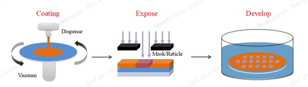
In the early 1980s, this process drew lines that were 3mu wide with visible light on a whole 4-in wafer at a time. In 2025, you draw 3text{nm} lines with Extreme Ultraviolet (EUV) rays, one section of a 10-in wafer at a time, but the principle is the same.
This is similar to photography. If you want to shoot an Ansel Adams-like landscape with objects near and far equally sharp, you use a narrow aperture with a long exposure time. If, on the other hand, you want to capture the sharp image of a performer in motion against a blurry background, you use a wide aperture with a short exposure time:

A silicon wafer is supposed to be flat, and depth of field not an issue. Real wafers, however, are slightly warped:

As a result of this warpage, increasing the aperture caused some of the lines to be blurry, and the attempt to increase capacity by increasing aperture crashed the yield instead.
Improving the Engineering Change Process
The engineering change procedure is not directly visible on the shop floor, but its output is. If you see work instructions that no one has updated in 5 years, you know it’s not working.
Because it involves production management, engineering, maintenance, quality, safety, and sometimes even a customer, the management of engineering changes is, perhaps, the most challenging part of manufacturing operations to improve. But its dysfunction in many factories makes it a bottleneck in quality improvement, and all the literature on quality says about it is that the number of engineering changes over time is a metric of process stability.
In our MES work at Fairchild, we eliminated the use of paper in engineering change management. We let engineers submit change requests to all reviewers simultaneously, rather than sequentially. They could then apply approved changes to wafers that were already in process, as we provided instructions in electronic form rather than hard copy. It was the “SpecEditor,” and my personal involvement with it was writing the user manual.
The engineers adopted the SpecEditor with gusto, but the managers failed to understand its benefits. In 1983, it was ahead of its time. We used a similar system called Code Management System (CMS) from DEC to organize our own software development, which inspired the SpecEditor. In software, the UNIX Source Code Control System (SCCS) later played the same role and, today, you can use Git.
Manufacturers were slower to recognize the value of revision management, and didn’t massively acquire software to do it until forced to do so for ISO-9001 certification, which doesn’t mean they understood its value. Today, these software functions fall under Master Data Management (MDM), which includes Product Data Management (PDM).
Beyond automating bureaucracy
While the SpecEditor sped up the administration of engineering changes, it did not change the method by which the organization processed them. It was a bureaucratic procedure, and the SpecEditor automated the bureaucracy.
The effectiveness and efficiency of an administrative procedure vary with the talent and attitudes of the people involved. A flood of half-baked requests, like a denial-of-service attack, can bring the best procedure to a standstill.
The more engineers vet their ideas upfront with other stakeholders, the faster their change requests turn into improved processes. Also, the less time reviewers spend denying flawed requests.
The change requests from engineers with a record of successful changes can receive reduced scrutiny. They pass the reviewers’ sleep-at-night test. The reviewers are not fretting all night over the consequences of decisions from trusted engineers.
A system like the SpecEditor facilitated the individual review process. A group of stakeholders, however, can review a request faster and more effectively in a meeting than individually. In an emergency, the manager in charge should have the authority to call an ad-hoc review meeting. If a process routinely has a flow of non-emergency engineering change requests, then it makes sense to hold regular meetings of a review panel for the engineers to argue for the approval of their proposals and get a decision.
QC Circles at Fairchild
I arrived at Fairchild at the peak of the QC circle fad in American industry. I was invited to QC circle leader training and attended several QC circle meetings. The following illustration is from the training materials we used, from Lockheed in 1977:

In principle, the company didn’t meet the conditions for QC circles to be successful. The operators had no job security. The supervisors of some of the participants had just told them to expect “a 20% headcount reduction.” Yet they participated with an eagerness I found astonishing.
The expectations were not clear. In particular, no one expected QC circles to enhance yields. They were not a topic of discussion at the plant I was working at. A few months later, a new management team took over the company and cancelled QC circles. Instead, they sent employees to Philip Crosy’s Quality College. There, they were not taught Ishikawa’s 7 tools. Instead, they learned to achieve Zero Defects by committing to “do it right the first time.”
This was my last experience of QC circles in an American factory that wasn’t a Japanese transplant. Almost 20 years later, I worked with NH circles at Honda in Ohio, a successful extension of QC circles.
The Quality Department
The quality department was not highly visible inside the wafer fabs. Outside, it played a role in customer relationships, negotiating specs and responding to quality problem reports. Contacts with its members introduced me to acronyms of World War II vintage, such as AQL, LTPD, AOQL, or ASN. These do not always mean what the words suggest.
AQL plans — Perceptions
AQL, for example, stands for “Acceptable Quality Limit.” Like everyone around me, I assumed that the AQL was an upper bound on the fraction defective of accepted materials. Suppose you took a sample from a lot and tested it according to a plan with an AQL of 1%. In that case, you would assume that passing a lot guarantees that it is less than 1% defective.
In 2025, the Wikipedia article on the topic still misstates the meaning of the AQL. ChatGPT also misleads you about the AQL. It says, “an AQL of 1% means that up to 1% of the items in the sample can be defective for the batch to still be considered acceptable.” The Velaction website provides resources for continuous improvement. On it, you read, “An acceptable quality level (AQL) is the percentage of defects allowed for a lot before it is rejected by a customer,” which, in addition, confuses “defects” and “defectives.”
AQLs — Reality
The AQL is, in fact, a characteristic of the inspection or test procedure. It is not a measure of outgoing quality. A sample inspection, or test, has an operating characteristic (OC) curve. It is a plot of the probability that a lot passes as a function of its fraction defective:

If a lot contains no defective, it has a 100% probability of passing; if all its units are defective, 0%. The OC curve shows how this probability varies with the percentage r of defectives in the lot. It is a mathematical calculation of the conditional probability Pleft ( text{Pass}| rright ) of passing, given r.
It doesn’t tell you about r. By definition, the AQL is the percentage of defectives at which the OC curve crosses 95%. It means that any lot with r leq text{AQL} passes at least 95% of the time. The AQL tells you nothing about failing bad lots. It is about the producer’s risk, not the customer’s.
LTPDs
The LTPD is another summary of the OC curve with a confusing name: “Lot Tolerance Percent Defective.” It is where the OC curve crosses 10%. A lot with r geq text{LTPD} fails at least 90% of the time. This is of greater interest to the customer.
This left me wondering why customers would show any interest in AQLs. It could only mean that they mistook them for acceptable quality limits and didn’t look under the hood.
Deming on Acceptance Sampling
In his 1986 book Out of the Crisis, Deming would bash the whole idea of acceptance sampling. He did not stop with the alphabet soup of acronyms. “The day of such plans,” he wrote, “is finished. American industry can not afford the losses that they cause” (p.133). Sampling was a domain that Deming knew well, having written a well-respected book about its theory. So, when he advocates against it, we should pay attention.
As we have seen, an AQL plan doesn’t protect the customer. Therefore, you shouldn’t use it to make decisions on accepting lots of parts. Sampling itself, however, is not always avoidable, for example, when the only way to validate a part is destructive testing.
Other Encounters
During this period, I also caught glimpses of quality practices in other industries through personal communications and participation in conferences.
Quality Sabotage
Long before, I had heard of American manufacturers designing products to fail as soon as the warranty expired. This sounded so perverse that I didn’t believe it. Then, at Fairchild, I met an older engineer. His whose first job for an appliance maker in the 1950s had been exactly that.
How could companies deliberately spend money to lower the quality of their products? But this man had done this kind of work and hated it. It was malicious, and it was corporate hubris at its worst. It created opportunities for competitors, which they eventually took. The manufacturer he had worked for was no longer in business.
The Great Lightbulb Conspiracy was another story of market disruption that I had heard of but disbelieved, until IEEE Spectrum published the details in 2014: the manufacturers of incandescent light bulbs conspired to reduce the lives of the bulbs.
The article gives dates, names, and places. The leading lightbulb manufacturers in the US, Germany, the Netherlands, France, and Japan set up the Phoebus Cartel in Geneva in 1924. Its goal was to reduce the lifespan of bulbs from 1,500 hours to 1,000 hours. And they stayed at this low level until LEDs made incandescent bulbs obsolete in the late 1990s.
I saw no such thing in semiconductors. Everyone was struggling to make better chips and bring the yields up. In mature industries in the US post-World War II, quality strategy had ranged from neglect to sabotage. By 1980, Japanese manufacturers in several key industries, like Toyota and Nissan in cars, or Sony in electronics, had taken advantage of it. They had used quality as a wedge to gain market share in the US and put a stop to these practices.
ASQC Congress, Baltimore, May 1985
Today, you cannot find anything about this event on the web. I remember it because it was the first time I spoke at a professional conference. I presented a mathematical model of the effect of rework on cycle time. It was also an opportunity to learn what was happening to quality outside of my semiconductor bubble. It shook my faith in the ability of the profession to make a difference in US manufacturing.
An engineer still in his twenties presented a project he had done in a factory. I don’t remember what the factory was making, but it was not high-technology. It was a textbook case application of SPC to solve a problem. There was nothing extraordinary about it other than his enthusiasm. No one had used these tools in that factory before. He concluded by describing the challenges he was facing in convincing management to support his work.
In 1985, the techniques he used had been around and promoted by the profession for 60 years. Yet they were still the object of missionary work. A basic application was worth presenting at a National Quality Congress. It made me think that, if these methods ever were to get any traction, they would have by then.the
At conferences, you often learn more in conversations with fellow participants during breaks than from the talks. They complained about conflicts between Production’s determination to ship units and Quality’s attempts to keep them from shipping defectives. That productivity and quality go together was a notion I had naively assumed everyone accepted.
Conclusions
In this complex industry, I had arrived with simple ideas. Whether under Quality Control, Quality Assurance, or Quality Management, it is a body of knowledge that claims universal applicability. My first experience was with an industry to which none of it applied.
The semiconductor industry, with its global sales of $5.4B in 1981, and manufacturing professionals dismissed it as marginal. In 2024, its sales were $630.5B (source:SIA). It is no longer small or marginal. Its products power not only electronic goods but also control cars, airplanes, household appliances, production machinery, etc. This makes its process and its approach to quality worth studying.
Each industry has its own customer expectations, business models, and challenges in management and technology that drive quality management. There is no one-size-fits-all approach that works.
#quality, #semiconductors, #yieldenhancement
August 28, 2025 @ 12:30 am
It is always a great pleasure to read about Michel Baudin’s experience and his lessons learnt. When he revisits a subject such as “quality” you learn a lot and it is very inspiring.
Merci Michel.